Department of Functional Materials
Carbon-Based Materials and Functional Films Laboratory
【Carbon-Based Materials and Functional Films Laboratory】
Carbon-Based Materials and Functional Films Laboratory is affiliated to Institute for Advanced Materials and Technology (IAMT) at University of Science and Technology Beijing (USTB), with four research specialist staff. The main research interests focus on Diamond and Related Materials as well as corresponding Technologies, including the preparation and process of large-scale high-quality free-standing diamond film, heat management of high-power device, new functional film and preparation technology, surface modification of thin film, advanced electrochemical water treatment technology, frictional and wear properties of hard thin films (nitrides, carbides, oxides) and ultra-nanocrystalline diamond, surface plasma alloying and plasma diagnosis, etc. Based on the applied science research, the laboratory combines basic material research with industrial application, they have completed many main projects, including National Key R&D Program of China, International Intergovernmental Cooperation Project (EU Horizon 2020, China-Russia Cooperation), National Major Defense Project, National Defense Innovation Pre-research and Supporting Project, National “863” Project, National Natural Science Foundation of China, as well as Provincial and Ministerial Level and Enterprise Cooperation Development Projects, etc. More than 300 publications and 70 authorized patents were authored. Recent years, they have built close relationship with University of Leicester (UK), Cork Institute of Technology (Ireland), Texas A&M University (USA), Argonne National Laboratory (USA), National Institute for Material Science (Japan), etc. Last three years, as a well-known research team with grown international influence, they have regularly visited famous universities and research institutes abroad, and they have also steadily received medium- and long-term foreign visiting scholars and exchange students.
【Lab members】
|
|
|
|
Li Chengming |
Tang Weizhong |
Wei Junjun |
Liu Jinlong |
Li Chengming Professor, Doctoral Supervisor
Tang Weizhong Professor, Doctoral Supervisor
Wei Junjun Associate Professor, Master Supervisor
Liu Jinlong Associate Professor, Master Supervisor
【The Main Research Focuses and Achievements of Laboratory】
1. Preparation and Processing of Large-scale High-quality Free-standing Diamond Film
The direct-current (DC) arc plasma jet CVD technology is a promising approach to synthesize large-scale high-quality diamond film with astonishing deposition rate. This technology has been built independently by them in a specific form for the preparation and process of large-scale high-quality free-standing diamond film at the age of early 1990s. Up to now, they have established a complete technique process system that integrating diamond deposition, shaped machining and precision polishing. The free-standing diamond film with thickness of 2 mm and diameter of 150 mm as well as surface roughness of less than 5 nm can be produced as optical window for the military and civilian application, or as cooling platform of high-power electronic devices, etc. Based on these achievements, many main projects including National Natural Science Foundation of China and Doctoral Program Foundation of the Ministry of Education, etc have been undertaken. They have authored over 80 academic publications, applied for one international invention patent and 20 domestic invention patents based on this research focus.
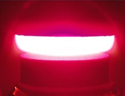
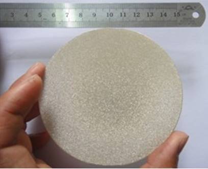
Figure.1 Photographs of the DC arc jet plasma CVD equipment (left) and deposited high-quality free-standing diamond film (right)
2. High-power microwave plasma chemical vapor deposition equipment (HP-MPCVD)
It is well known that high-power microwave plasma chemical vapor deposition is the preferred approach to synthesize high-quality diamond film. Aiming at the urgent demand of high grade diamond film, the Laboratory has broke through the high-power MPCVD equipment technique and developed several 2.45 GHz and 10 kW MPCVD equipments for diamond deposition. One of the newly built system was designed in an all-new structure scheme as shown below. It can be operated for a long period time at 10 kW to deposit high-quality diamond film with supreme purity and significant reduction of nitrogen or silicon contaminations. Currently, this mentioned equipment is being used for high grade diamond film deposition.
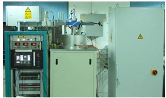
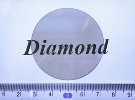
Figure.2 The 2.45 GHz and 10 kW MPCVD system (left) and deposited optical grade diamond film (right)
3. Thermal management of diamond-based ultra-high thermal flux density system
The highest thermal conductivity is one of unique properties of diamond. Therefore, the diamond-based thermal management system with ultra-high thermal flux density is considered worldwide as the most effective way to cool electronic devices down. Using finely processed thick diamond plate with over 3 mm thickness and thermal conductivity >1500 W/mK, the heat conduction and heat dissipation can be realized at the same time to enhance the thermal bearing capacity with increased heat flux of 1000 W/cm2. As shown in Figure.3, it is the diamond heat-dissipation plat component of high-performance electronic device system with excellent temperature reduction and uniform heat distribution, of which the cooling substrate was fabricated by the thick free-standing diamond film. Moreover, the dissipating heat flux density of the efficient pump-driving two phases fluid loop evaporator can be more than 500 W/cm2 based on the diamond micro channels with high aspect ratios. They are still working on the deeper system research concerning the diamond micro-nano machining, hear transfer compatibility of diamond, thermophysical property improvement of heat transferring media.
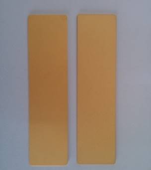
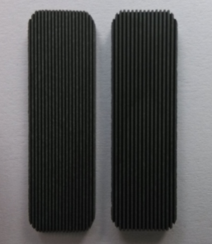
Figure.3 Photographofdiamond heat-dissipation plat component of high-performance electronic device system (left) and thick diamond plate with surface microchannels (right)
4. Technical research of high-quality single crystal diamond
CVD single crystal diamond (SCD) can be introduced for many advanced technology applications, e.g., wide-gap semiconductor, radiation detector, high pressure physical experiment, ultra-fine process, owing to the intrinsic characteristics especially the absence of grain boundary and controllability of impurity. The Lab team has synthesized large high-quality single crystal diamond with 10mm×10mm× 5mm and impurity content < 100 ppb based on the homoepitaxial technology. The ongoing SCD related researches include key technology of multi-seeds high-quality CVD homoepitaxial growth, post-treatment and surface modification, CVD SCD radiation detector application, high pressure physical investigation, ultra-fine process of CVD SCD and decoration application, etc. These researches were supported by National Natural Science Foundation of China and International Cooperation Project of the Ministry of Science and Technology, etc.
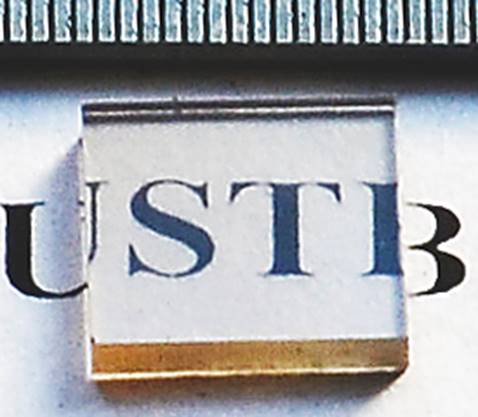
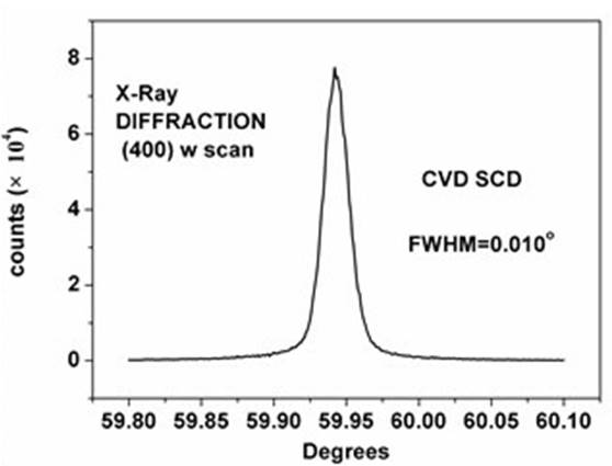
Figure.4 A large-size CVD single crystal diamond (left) and its X-ray diffractionpattern (right)
5. CVD diamond radiation detector
Diamond can be used as radiation materials in extremely harsh environment owing to its outstanding radiation resistance nature. Compared with other available radiation materials, diamond has many superior properties such as high electrical resistivity, low dielectric constant, which guarantee the low noise and high signal-noise ratio of radiation devices. Meanwhile, the high break down voltage and excellent carrier mobility of diamond make diamond-based radiation detector operate under high voltage with good charge collection efficiency and fast time response. In addition, owing to the very close atomic number to the equivalent atoms of human soft tissue associate with the non-toxic as well as non-reactive nature with organism, diamond is an ideal material for fabricating body-internal radiation does detector. They have successfully fabricated high-quality SCD radiation detector andinvestigated its dark current. The results indicated the low dark current is located within the favorable level for the application of radiation device, which promoted the further high-performance radiation detector research. This topic was supported by the International Cooperation Project of Ministry of Science and Technology of China.
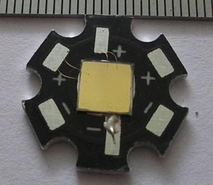
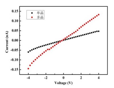
Figure.5 The fabricated single crystal diamond radiation detector (left) and its I-V curve of dark current (right)
6. Diamond-based Metal-Oxide-Semiconductor Field Effect Transistors (MOSFETs)
With the development of communication technology towards extremely high frequency and very large capacity, it is required that the key components of communication satellites, such as signal receiving and transmitting terminal, work at extremely high frequency and very large power. At this situation, the traditional semiconductor materials such as Si, GaAs and so on are difficult to meet the requirement.Due to its wide band gap, high carrier mobility, low dielectric constant, high Johnson index and Keyes index, diamond material has become the best material choice for ultra-high frequency and ultra-high-power applications, it thus is also known as the fourth-generation semiconductor material. They kept pace with the forefront of international research hot spot, for example, the hydrogen terminated diamond surface conducting channel of the surface of the carrier transport properties and the conductive mechanism were studied in-depth. Based on the hydrogen terminated surface of diamond, the p-type conductive channel diamond-based field effect transistor electronic device was developed in domestic, and its performances are leading at the domestic. As a fourth-generation semiconductor, diamond's high thermal conductivity associate with its excellent performance of high temperature and high-pressure resistance enables it to meet the application need of ultra-high frequency and ultra-high-power field.This research field is supported by the National Natural Science Foundation of China, the China Post-doctoral Science Foundation, and the State Key Laboratory of Specialized Integrated Circuits Foundation.


Figure.6 Diamond-based MOSFET (left) and its frequency characteristic (right)
7. Diamond-based surface acoustic wave (SAW) devices
Diamond has the highest sound propagation speed and the highest young's modulus among all the known materials. Meanwhile, it has high thermal conductivity and excellent heat resistance. It is recognized as the most promising material for new high-power, high-frequency and high-performance surface acoustic wave devices. Laboratory members have successfully deposited 4 inches diamond film with 20 microns thickness on silicon by employing the home-build DC arc plasma jet CVD, and then prepared SiO2/ZnO/Diamond/Si multilayer structure by depositing SiO2 and ZnO using coating system, on the basis of making a interdigital electrode structure and the surface acoustic wave devices was finally fabricated. The center frequency of this device was up to 2.63 GHz with as high as the velocity of 10520 m/s and 3 dB bandwidth of 333 MHz. The electromechanical coupling coefficient was 0.6%, and the insertion loss was 34.43 dB. The device was expected to be commercially produced after further optimization. This research was supported by the 863 Program and the China Postdoctoral Science Foundation.
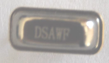
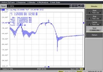
Figure.7 Diamond-based surface acoustic wave (SAW) device (left) and its frequency response (right)
【The Main Scientific Research Projects of Laboratory】
1. International Cooperation Project of Ministry of Science and Technology of China, Diamond-based nanomaterials and nanostructures for advanced electronic and photonic applications, 4.36 million, 2017-2020;
2. International Cooperation Project of Ministry of Science and Technology of China, Cooperative research on a new high energy particle detector with diamond structure, 900 thousand, 2014-2017;
3. National Magnetic Confinement Nuclear Fusion Energy Development Research Special Project,Study on key technology of megawatt cascade pulsed gyrotron, 500 thousand, 2013-2015;
4. National Key Research and Development Program, Preparation and photoelectric properties of semiconductor diamond materials, 720 thousand, 2018-2020;
5. National Natural Science Foundation of China, Study on the formation and stability mechanism of carrier transport channel on hydrogen terminated diamond surface, 250 thousand, 2015-2017;
6. National Natural Science Foundation of China, Mechanism of enhancement of diamond film strength by argon plasma arc treatment, 800 thousand, 2013-2016;
7. Innovation Research Project of Ministry of National Defense of the P.R. China, 2.7 million, 2016-2020;
8. Pre-research project of Ministry of National Defense of the P.R. China, 2 million, 2017-2020;
9. Pre-research project of Ministry of National Defense of the P.R. China, 900 thousand, 2016-2018;
10. Pre-research foundation of Ministry of National Defense of the P.R. China, 400 thousand, 2017-2019;
11. CAST foundation, High efficiency heat transfer technology and fluid mechanical wear reduction technology based on nanometer graphene, 900 thousand, 2016-2018;
12. State key laboratory foundation of China, Study on the surface growth diamond film technology of GaN, 320 thousand, 2017-2018;
13. Enterprise cooperation project, approximately 10 million, 2016-2020.


