
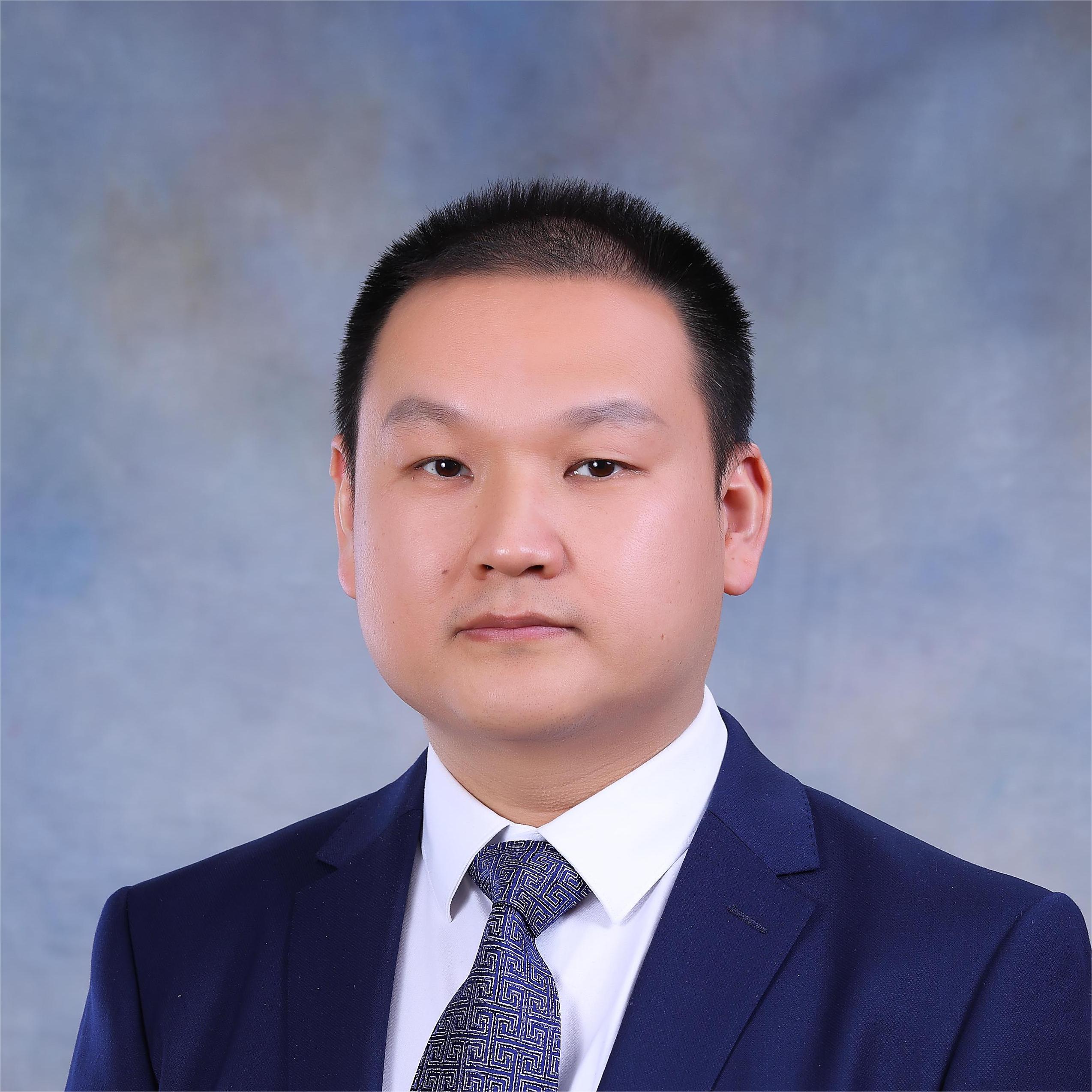
魏俊俊
姓名:魏俊俊
所在系所:功能材料研究所
职称:研究员
通信地址:北京市海淀区学院路30号北京科技大学新材料技术研究院
邮编:100083
办公地点:金物楼208
办公电话: 010-62332475
邮箱:weijj@ustb.edu.cn
个人简介
研究方向
科研业绩
代表性论文
[1]. Y. Li, H. Li, C.M. Li, J.J. Wei*. A review of the study of diamond NV color centers: fabrication, application and challenge. Functional Diamond, 2025, 5(1):2567286.
[2]. J.X. Zou, Z. Chang, W.Z. Leng, L.P. Zheng, P. Liu, J.J. Zhang, L.X. Chen, J.L. Liu, C.M. Li, J.J. Wei*. A high-efficiency polishing strategy for polycrystalline diamond: synergistic effects of plasma pretreatment and short-duration chemical mechanical polishing. Diamond & Related Materials, 2026, 167:113902
[3]. Y.T. Zheng, Q.R. Zhang, G.Z. Qiao, J.J. Wei*, et al. Preparation strategy for low-stress and uniform SiC-on-diamond wafer,A silicon nitride dielectric layer[J],Ceramics International,2022, 48(24):36441-36449.
[4]. J.L. Tu, J.D. Shi, L.X. Chen, J.L. Liu, C.M. Li, J.J. Wei*. Surface termination of the diamond microchannel and single-phase heat transfer performance[J],International Journal of Heat and Mass Transfer,2022, 199: 123481
[5]. J.J. Wei, D.H. Jing, H. Li, et al. Efect of heat treatment on fuorescence characteristics of HPHT and detonation nanodiamonds[J]. Nanoscience, 2022, 12(11):3449-3457.
[6]. X.B. Yan, J.J. Wei*, K. An, et al. High temperature surface graphitization of CVD diamond films and analysis of the kinetics mechanism[J]. Diamond and Related Materials, 2021,120:108647.
[7]. Y.F. Liang, Y.T. Zheng*, J.J. Wei*, et al. Effect of grain boundary on polycrystalline diamond polishing by high-speed dynamic friction [J]. Diamond and Related Materials, 2021, 117: 108461.
[8]. 6. X.B. Yan, J.J. Wei*, K. An, et al. Graphitization of CVD diamond grain boundaries during transient heat treatment [J]. Diamond and Related Materials, 2021, 116: 108433.
[9]. X. Jia, J.J. Wei*, Y.B. Huang, et al. Fabrication of low stress GaN-on-diamond structure via dual-sided diamond film deposition[J]. Journal of Materials Science, 2021, 56: 6903-6911.
[10]. Z.N Qi, Y.T.Zheng, J.J. Wei*, et al. Surface treatment of an applied novel all-diamond microchannel heat sink for heat transfer performance enhancement[J], Applied thermal engineering, 2020, 177: 115489.
[11]. Z.N Qi, Y.T.Zheng, X.H. Zhu, J.J. Wei*, et al. An ultra-thick all-diamond microchannel heat sink for single-phase heat transmission efficiency enhancement[J], Vacuum, 2020, 177: 109377.
[12]. X. Jia, J.J. Wei*, Y.B. Huang, et al. Enhancement of diamond seeding on aluminum nitride dielectric by electrostatic adsorption for GaN-on-diamond preparation[J]. Journal of Materials Research, 2020, 35(5): 1-8.
[13]. X. Jia, J.J. Wei*, Y.C. Kong, et al, The influence of dielectric layer on the thermal boundary resistance of GaN-on-diamond substrate[J], Surface and Interface Analysis, 2019, 51(7):783-790.
[14]. J.J. Wei, X.Y. Zhu, L.X. Chen, et al, High quality anti-sticking coating based on multilayer structure[J], Surface and Coatings Technology, 2019, 362:72-77.
[15]. X.B. Yan, J.J. Wei*, K. An, et al, Quantitative study on graphitization and optical absorption of CVD diamond films after rapid heating treatment[J], Diamond and Related Materials, 2018, 87: 267-273.
[16]. X.B. Yan, J.J. Wei*, J.C. Guo, et al, Mechanism of graphitization and optical degradation of CVD diamond films by rapid heating treatment[J], Diamond and Related Materials, 2017, 73: 39-46.
参编专著
[1] 《金刚石膜制备与应用》,科学出版社(978-7-03-041822-7),2014.08
[2] 《Novel aspects of diamond Ⅱ-Science and Technology》, Springer Nature(978-3-031-47556-6), 2024.06
[3] 《Diamond Technology and Advances》,The Royal Society of Chemistry, 2026
已授权专利
[1] 魏俊俊,邹金鑫,冷王喆等,一种基于两步zeta电位调控的多晶金刚石化学机械抛光方法,发明专利,ZL202411841870.1
[2] 魏俊俊,叶盛,赵上熳等,一种通过多重激光快速平整金刚石膜的方法,发明专利,ZL202410077617.7
[3] 魏俊俊,朱芬,黄毅丹等,一种增强高功率电子器件辐射散热的界面材料的制备方法,发明专利,ZL202410640935.X
[4] 魏俊俊,乔冠中,王越等,一种低界面热阻金刚石基晶圆及其低温键合方法,发明专利,ZL202210482785.5
[5] 魏俊俊,王越,乔冠中等,一种具有金刚石钝化层的TaN薄膜电阻器的制备方法,发明专利,ZL202211163967.2
[6] 魏俊俊,涂军磊,史佳东等,一种歧管式全金刚石微通道散热器的制备方法,发明专利,ZL202110419168.6
[7] 魏俊俊,史佳东,涂军磊等,一种快响应超黑材料及其制备方法,发明专利,ZL202110159705.8
[8] 魏俊俊,黄亚博,陈良贤等,一种带光学增透膜的金刚石制备方法,发明专利,ZL202011158364.4
[9] 魏俊俊,荆豆红,梁毅凡等,一种基于催化反应减小纳米金刚石粒径的方法,发明专利,ZL202010519160.2
[10] 魏俊俊,李成明,陈良贤等,一种金刚石基薄膜电阻元件的制造方法,发明专利,ZL201910459340.3
[11] 魏俊俊,齐志娜,李成明等,一种超高热流密度散热用金刚石微通道热沉的制备方法,发明专利,ZL201810487436.6
[12] 魏俊俊,吴晶恩,李成明等,一种高导热片-金属热沉界面热阻测量装置及方法,发明专利,ZL201810009990.3
[13] 魏俊俊,贾鑫,李成明等,一种采用双金刚石层实现GaN原始衬底转移的方法及应用,发明专利,ZL201811340254.2
[14] 魏俊俊,李成明,刘金龙等,一种表面P型导电金刚石热沉材料的制备方法,发明专利,ZL201510623007.3;
[15] 魏俊俊,李成明,黑立富等,一种研磨抛光机的磨料自动添加装置,发明专利,ZL201310150661.8;
代表性奖励:
[1] 北京市科技进步二等奖,排名第1
[2] 中国材料研究学会科技进步一等奖,排名第1
[3] 十一届国际发明展览会金奖,排名第1
[4] 中国发明协会发明创业项目一等奖,排名第1
[5] 生产力促进创新发展一等奖,排名第1